Table Of Content

By grouping components logically and considering the accessibility for soldering and testing, manufacturers can reduce assembly time and minimize the risk of errors or rework. Printed circuit boards (PCBs) are ubiquitous in electronics and make up a substantial fraction of environmentally hazardous electronic waste when devices reach end-of-life. Their recycling is challenging due to their use of irreversibly cured thermoset epoxies in manufacturing. Here, to tackle this challenge, we present a PCB formulation using transesterification vitrimers (vPCBs) and an end-to-end fabrication process compatible with standard manufacturing ecosystems.
PCB Layout Design
One of the key concepts in electronics is the printed circuit board or PCB. It's so fundamental that people often forget to explain what a PCB is. This tutorial will breakdown what makes up a PCB and some of the common terms used in the PCB world. Once the schematic sets the stage, the next step in the journey of creating a Printed Circuit Board (PCB) is to simulate the circuitry. It allows engineers to verify the functionality of the circuit before investing time and resources in manufacturing. By identifying and rectifying any design flaws or errors in the simulation stage, costly mistakes can be avoided.
Impedance Matching and Termination
Minimize the number of vias and keep them away from high-speed signal paths to reduce signal reflections and losses. Double-sided PCBs have conductive traces and components on both sides of the substrate, connected using through-hole vias. These vias are drilled holes plated with conductive material, allowing electrical signals to pass between layers. Double-layer PCBs offer more complex routing and higher component density compared to single-sided boards, making them suitable for various applications, from consumer electronics to industrial control systems.
Printed circuit boards made greener
There are several options available, both free and paid, that provide a user-friendly interface and a wide range of features. Some popular choices include Eagle, Altium Designer, KiCad, and OrCAD. Consider your specific requirements, budget, and level of expertise when selecting the software that best suits your needs.
PCB Design: A Comprehensive Guide to Printed Circuit Board Design - Part 1
If your board checks out, then you’re ready to release your manufacturer deliverables. A traffic light PCB layout is a printed circuit board that controls the operation of traffic lights. It is designed to ensure that the traffic signals operate correctly and safely, allowing vehicles and pedestrians to move through intersections without incident. Rigid-flex PCBs are a combination of rigid and flexible PCBs, integrating both types of substrates into a single board.
Step 2: Create a Blank PCB Layout
The Importance of Test Points in Circuit Design - Electronic Design
The Importance of Test Points in Circuit Design.
Posted: Wed, 13 Dec 2023 08:00:00 GMT [source]
In 1943, the Austrian Paul Eisler, working in the United Kingdom, patented a method of etching the conductive pattern, or circuits, on a layer of copper foil attached to a hard base that did not conduct electricity. Eisler's technique was noticed by the US military and they started to use it in new weapons including proximity fuzes in World War II. His idea became very useful in the 1950s when the transistor was introduced. Up to that point, vacuum tubes and other components were so large that the traditional mounting and wiring methods were all that was needed. With the introduction of transistors, however, the components became very small, and manufacturers needed to use printed circuit boards so the connections could also be small.
As a general guideline, try to allow 0.350” – 0.500” of spacing between each of your ICs, and even more space for larger parts. Be sure to orient all of your components of a similar type in the same direction. This will help your soldering process go off without a hitch as your board rolls through the soldering oven.
First, create a blank printed circuit board document which will generate a PcbDoc file. Not only is circuit interconnectivity easier to define and edit, but converting a schematic to a circuit board layout is much easier than designing directly on the board. For components, Altium Designer has an extensive database of parts libraries.
Recyclable vitrimer-based printed circuit boards for sustainable electronics
By following a well-defined PCB design workflow and fostering collaboration between different teams, designers can create high-quality, reliable, and manufacturable PCBs that meet the specific requirements of the application. The final step in the PCB design workflow is the generation of manufacturing files, such as Gerber files and drill files, which are used by the PCB fabrication house to produce the physical boards. The manufactured PCBs then undergo testing and assembly before being integrated into the final electronic product.
You need to consider components as well as the routing of connections. Make sure never to design a circuit board layout where connections have to cross, as this can cause an overlap in signals that may ruin your design. Luckily for you, the experts here have outlined some of the most critical parts of printed circuit board layout so that you don’t have to go it alone. This guide will show you some essential tips and tricks to remember when designing a PCB. The fabrication and assembly processes for these types of PCBs vary, but today's ECAD software can help designers create any of these boards as long as the right PCB design rules are enforced in the software.
Larger vias and more closely spaced vias can provide better thermal conductivity, but may also impact signal integrity and routing density. Placing thermal vias directly under high-power components, such as processors or power regulators, can help provide a direct thermal path to the PCB's exterior. Part one establishes a strong foundation, exploring the design workflow – from schematic capture to layout and crucial design rule checks. We'll examine PCB components and layers, then examine signal integrity and thermal management – essential for crafting high-performance PCBs. The knowledge, skill set, and experience required to be successful in PCB design has evolved into what is known today as printed circuit engineering. This evolution requires a comprehensive understanding for design of packaging solvability, performance, and manufacturing.
In conclusion, creating a functional and reliable PCB requires a comprehensive understanding of design principles and best practices. This includes careful consideration of factors like component selection, placement, and routing, as well as adherence to manufacturability guidelines. By following a structured workflow that incorporates schematic design, PCB layout, and rigorous verification steps, designers can ensure the integrity and performance of their PCBs. Signal integrity, electromagnetic compatibility, and thermal management are crucial aspects to consider while designing PCB. This knowledge empowers engineers to develop innovative and functional electronic devices that play an integral role in modern technology.
[2] Its glass transition temperature (Tg) ranges from 130°C to 180°C, with a thermal conductivity of 0.3 W/mK. The schematic serves as a blueprint for the PCB design process, helping engineers understand the circuit’s functionality. Unlike resistors, which are used to hamper the current and charge in circuits, transistors are used to amplify the current in a circuit. Once the “control current” flows through the transistor, a larger “main current” flows through it depending on which state it is in.
The specific details of the process may vary depending on the design of the board and the requirements of the application. A. Heat dissipation can be managed through proper component placement, the use of thermal vias and planes, and the selection of appropriate PCB materials. Thermal simulation tools can also be used to identify hot spots and optimize the thermal design. A. A single-sided PCB has components and traces on only one side of the board, while a double-sided PCB utilizes both sides for component placement and routing. Heat sinks are another effective tool for thermal management in PCB design.
The most common circuit boards are made in large numbers for a specific job, for example to run a computer, a mobile/cell phone or a television. Some circuit boards are made plain so a person can build their own for a new electrical task. Most things that use electricity have at least one circuit board inside of them that makes them run.
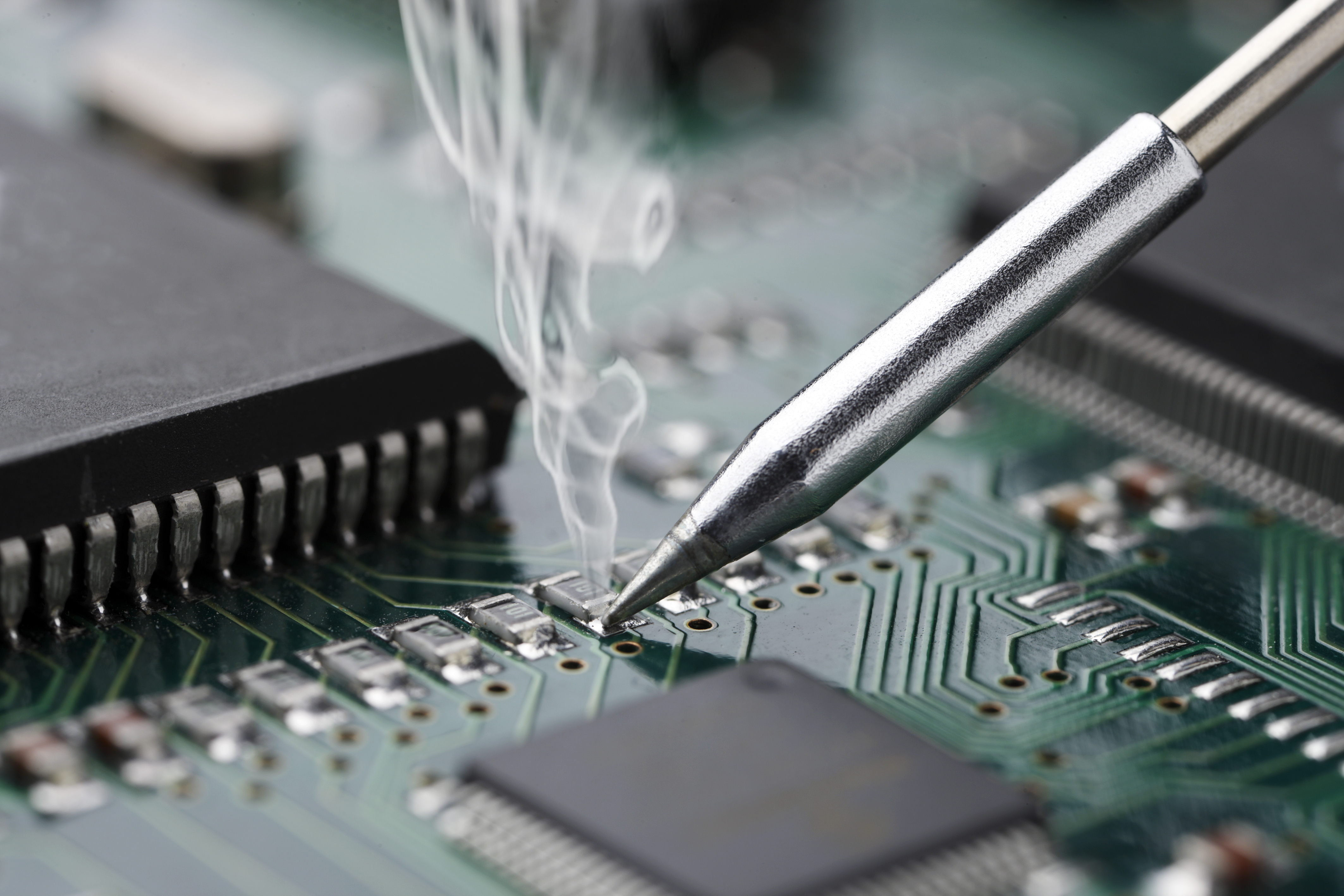
After these fabrication steps are completed, the bare board is sent into printed circuit board assembly, where components are soldered to the board and the PCBA can be tested. Once it comes time to lay out your circuit board, you’ll need to adopt a methodology that ensures your signals remain free of common problems, your board is manufacturable, and that you have followed important design rules. The right PCB design software with design rule checking features throughout the schematic and layout phases will help ensure your printed circuit boards can be manufactured properly and will function as designed. You can take advantage of the functionality and power of PCB design software applications—such as Altium Designer—to create advanced printed circuit designs with ease.


No comments:
Post a Comment